Trusting a Liar: How Your Breadboard Is Setting Your Prototype Up to Fail
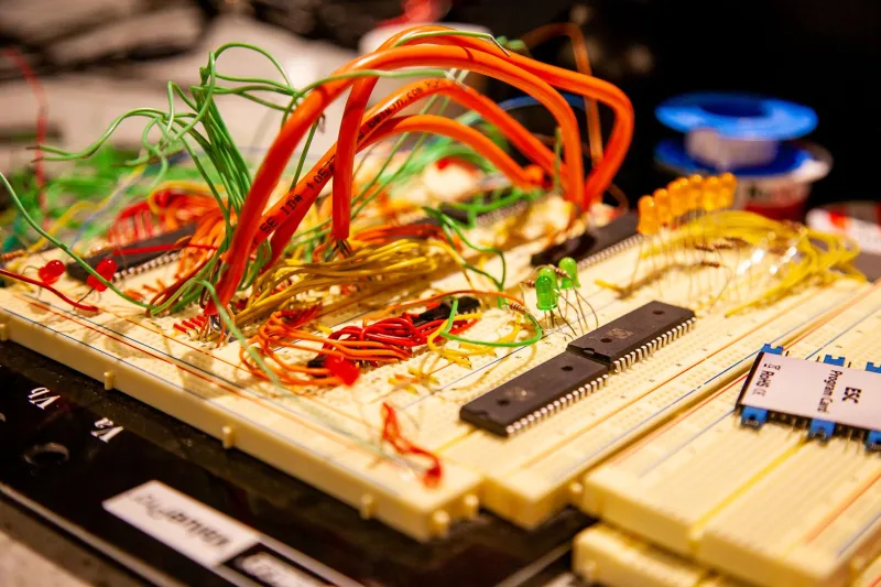
There is a certain comfort in the breadboard. Rows of neatly spaced tie points, the satisfying click of a component lead seating into a clip, the ease of rerouting a signal with a single wire pull — it is the sandbox every electronics student learns in and the rapid-iteration tool that professionals return to again and again. But that comfort carries a cost that rarely appears in any datasheet, lab manual, or introductory course: the breadboard is an electrically imperfect medium, and it will routinely lie to you about how your circuit actually performs.
This is not a criticism of the tool itself. The solderless breadboard is genuinely invaluable for low-frequency, low-speed design work. The problem arises when engineers — from first-semester students in university labs to seasoned professionals under deadline pressure — treat breadboard validation as a sufficient substitute for real-world circuit behavior. It is not. And the consequences of that misplaced trust can range from frustrating rework cycles to expensive, catastrophic production failures.
The Physics of the Problem
Every electrical connection in a breadboard introduces parasitics — unwanted passive elements that exist because of the physical geometry of the conductors involved. The spring-loaded clips that grip component leads are not ideal conductors. Each one contributes a small but measurable contact resistance, typically between 1 and 10 ohms depending on clip age, oxidation, and how firmly the lead seats. In a low-impedance power circuit, that resistance is negligible. In a precision analog signal path or a high-gain amplifier stage, it can shift bias points, introduce noise, and alter gain characteristics enough to make a design appear fundamentally flawed when it is actually sound — or, more dangerously, appear functional when it is not.
Inductance is the more insidious culprit. The long conductive strips running the length of a breadboard, combined with the wire jumpers engineers use to connect sections, form inductors. At audio frequencies, these parasitic inductances are inconsequential. But as operating frequencies climb into the megahertz range — as they do in switching power supplies, RF circuits, high-speed digital logic, and microcontroller-driven peripherals — the inductive reactance becomes significant. A breadboard connection that measures nearly zero ohms at DC can present tens of ohms of impedance at 50 MHz. The circuit that seemed stable at low frequencies begins to oscillate, ring, or fail entirely.
Capacitive coupling between adjacent rails compounds the issue. The parallel conductive strips in a standard breadboard are physically close together, creating distributed capacitance that can couple signals between ostensibly isolated circuit sections. In high-frequency analog designs, this coupling introduces crosstalk. In digital circuits, it can produce glitches on signal lines that a logic analyzer will flag as timing violations — violations that vanish entirely when the circuit is transferred to a proper PCB layout.
Real Failure Modes Engineers Have Encountered
Consider a scenario familiar to anyone who has designed switching power supply controllers: a prototype that regulates beautifully on the breadboard at light load, only to exhibit severe output voltage ripple and thermal runaway when the same design is assembled on a PCB. The breadboard's parasitic inductance in the feedback network altered the phase margin of the control loop just enough to appear stable under the limited bandwidth of a basic oscilloscope probe. The PCB, with tighter layout and lower parasitics, revealed the instability that was always present but masked on the bench.
A similar failure pattern appears frequently in RF work. Hobbyists building software-defined radio front ends or low-noise amplifiers on breadboards often report that their circuits perform 10 to 20 dB worse than simulations predict. The culprit is almost always the combination of parasitic inductance in the component leads and the capacitive loading of the breadboard strips — both of which detune matching networks and degrade noise figure. The design is not wrong. The test environment is simply incapable of representing it accurately.
Digital designers encounter their own version of this problem. High-speed microcontrollers, FPGAs operating above 50 MHz, and even modern ARM-based development boards can exhibit intermittent faults, memory corruption, or communication failures when prototyped on a breadboard. The signal integrity degradation introduced by the breadboard's parasitics — combined with the impossibility of achieving proper ground planes and controlled impedance traces — creates an environment where the chip's electrical specifications are violated even when the schematic is entirely correct.
Techniques for Validating What the Breadboard Actually Tells You
None of this means abandoning the breadboard. It means using it intelligently, with an awareness of its limitations.
For any circuit operating above roughly 1 MHz, treat breadboard results as directionally useful but not definitive. Use the breadboard to verify basic functionality, component selection, and gross topology — then transition to a PCB for real performance validation. Tools like KiCad, EasyEDA, and Altium offer free or low-cost entry points for hobbyists and students, and rapid-turnaround PCB fabrication services such as OSH Park and PCBWay have made small-batch prototyping accessible at a price point that was unimaginable a decade ago.
When breadboard testing is unavoidable at higher frequencies, minimize wire length aggressively. Use component leads trimmed as short as safely possible. Keep bypass capacitors physically adjacent to power pins rather than routing them through long breadboard traces. Add a proper ground plane by attaching a copper-clad board beneath the breadboard and using short jumpers to connect all ground nodes to it — this single modification dramatically reduces parasitic inductance in the ground return path and can make RF circuits behave far more predictably.
For power electronics work, measure not just output voltage but also switch node waveforms with a proper oscilloscope probe, looking specifically for ringing, overshoot, and oscillation that a multimeter will never reveal. If you observe behavior that changes when you physically move wires, apply pressure to connections, or vary ambient temperature, your breadboard contacts are telling you something important: the circuit's performance is sensitive to contact resistance, and no amount of further breadboard iteration will resolve that.
Knowing When to Stop Iterating and Start Laying Out
Perhaps the most important practical skill in prototype development is recognizing the transition point — the moment at which continued breadboard iteration yields diminishing returns and introduces more confusion than clarity.
A useful rule of thumb: if your circuit contains any switching element operating above 500 kHz, any RF signal path, any precision analog stage with gain above 40 dB, or any high-speed digital interface, the breadboard is the wrong validation tool. Use it for initial smoke testing and basic continuity, then move to PCB as quickly as possible. The time spent on a proper layout is nearly always recovered in the debugging time it saves.
For students particularly, this represents an important mindset shift. The breadboard is not the destination — it is the first step of a longer journey. Learning to recognize its limitations, and developing the PCB layout skills to move beyond it, is what separates a hobbyist who builds interesting demonstrations from an engineer who ships reliable products.
The breadboard will continue to occupy a central place on workbenches everywhere. Used with clear eyes and appropriate skepticism, it remains one of the most productive tools in electronics development. But it is a tool that works best when you understand exactly what it cannot tell you — and when you know better than to take its word for it.