Matched or Mismatched: Why Impedance Remains the Most Underestimated Variable in Modern Circuit Design

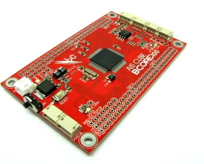
Photo: Taitamtinh, Public domain, via Wikimedia Commons
Ask any seasoned RF engineer about the most humbling moment of their early career, and there is a reasonable chance it involves a transmission line that behaved nothing like the simulation predicted. The math checked out. The schematic looked clean. Yet the output signal was attenuated, distorted, or riddled with reflections that no amount of component swapping seemed to resolve. The culprit, more often than not, was impedance mismatch — a problem deceptively simple to describe and notoriously difficult to solve in practice.
Impedance matching is not a niche concern reserved for RF specialists. It surfaces in audio amplifier design, USB signal integrity, antenna systems, sensor interfaces, and virtually every domain where a signal travels from one circuit element to another. Despite its ubiquity, it remains one of the most poorly understood concepts across engineering disciplines, not because the theory is inaccessible, but because the gap between theoretical understanding and applied intuition is wider than most textbooks acknowledge.
Why the Theory Alone Is Insufficient
At its core, impedance matching is straightforward: maximum power transfers from a source to a load when the source impedance equals the complex conjugate of the load impedance. In purely resistive systems at low frequencies, this reduces to matching resistances. For AC circuits, reactive components — capacitance and inductance — introduce phase shifts that complicate the relationship significantly.
The trouble begins when engineers apply these principles to real hardware. Textbook examples typically present idealized, frequency-independent components. Actual resistors carry parasitic inductance. Capacitors exhibit equivalent series resistance. PCB traces behave as distributed transmission lines above certain frequencies. A 50-ohm termination resistor that performs admirably at 10 MHz may present a substantially different impedance at 500 MHz, undermining the entire matching strategy.
This frequency dependence is the first major source of confusion. Engineers who design a matching network using lumped-element calculations and then build it on a PCB without accounting for trace geometry, via inductance, or component self-resonance frequently discover that their carefully designed network provides acceptable performance only across a narrow slice of the intended operating band.
The Transmission Line Problem
High-speed digital design has forced the transmission line conversation into domains that once considered it irrelevant. When signal rise times fall below approximately one-sixth of the propagation delay along a PCB trace, that trace must be treated as a transmission line — not a simple wire. For modern logic families switching in the sub-nanosecond range, this threshold is crossed on traces as short as an inch or two.
Unterminated transmission lines produce reflections. A signal launched down a 50-ohm trace that encounters a 100-ohm load will see a portion of its energy reflected back toward the source. That reflection then re-reflects if the source impedance is also mismatched, creating a standing wave of glitches, overshoots, and ringing that can corrupt data, trigger false logic transitions, or generate unintended electromagnetic emissions.
Series termination — placing a resistor equal to the difference between the driver's output impedance and the characteristic impedance of the trace — is among the most common remedies. Parallel termination at the load end is another approach, though it draws continuous current and may be inappropriate in power-sensitive designs. Differential pairs require matched impedances on both conductors simultaneously, adding another layer of geometric precision to the PCB layout process.
The critical insight that separates competent designers from struggling ones is this: termination strategy cannot be an afterthought. It must be embedded in the design from the earliest schematic stage, with PCB stack-up, trace width, and component placement all considered as interdependent variables.
RF Matching Networks: Where Small Errors Become Large Problems
In radio frequency design, impedance matching takes on additional complexity because antenna impedances vary with frequency, physical environment, and proximity to other objects. A dipole antenna presents a nominally 73-ohm impedance at its resonant frequency, but that value shifts considerably as operating frequency deviates from resonance or as the antenna is mounted near a conductive surface.
The Smith Chart — a graphical tool developed by Phillip Smith at Bell Labs in the 1930s — remains one of the most powerful instruments for visualizing impedance transformation across frequency. Engineers who invest the time to develop fluency with Smith Chart navigation gain the ability to design matching networks intuitively, tracing impedance loci through L-networks, pi-networks, and T-networks with a facility that purely numerical methods cannot replicate.
Vector network analyzers (VNAs) have become increasingly accessible to individual engineers and small teams, with capable instruments now available below the $500 price point. Devices such as the NanoVNA, while limited in dynamic range compared to professional laboratory equipment, provide sufficient accuracy for many amateur and educational applications. The ability to measure S-parameters — specifically S11 for return loss and S21 for insertion loss — and display them on a Smith Chart gives designers immediate, actionable feedback about where their matching network is succeeding and where it is falling short.
Common Troubleshooting Scenarios
Consider a practical scenario: an engineer designs a low-noise amplifier (LNA) intended to operate at 2.4 GHz. Simulation shows excellent noise figure and gain. On the bench, however, gain is several decibels lower than expected, and the noise figure is unacceptable. A VNA measurement of the input network reveals that the matching network, which was designed using component values extracted from a datasheet, is providing optimal impedance transformation at 2.1 GHz rather than 2.4 GHz. The shift results from parasitic capacitance in the PCB via connecting the matching network to the amplifier's input pin — a parasitic element absent from the simulation model.
The fix requires either adjusting the matching component values to compensate for the parasitic or redesigning the PCB layout to minimize via length. Neither solution is apparent without measurement, which underscores a broader lesson: simulation is a starting point, not a final answer.
Another common scenario involves audio amplifier output stages, where engineers sometimes neglect the reactive component of the load impedance. A loudspeaker does not present a flat 8-ohm impedance across its operating range. Its impedance varies substantially with frequency, reaching peaks at resonance that can be several times the nominal value. An amplifier optimized for resistive loads may behave erratically when driving a reactive speaker load, particularly at frequencies where the phase angle of the load impedance is significant.
Building Genuine Competence
Mastery of impedance matching is not achieved through memorization of formulas. It develops through iterative practice: designing matching networks, building them, measuring the results, diagnosing discrepancies, and refining the approach. Engineers who regularly use VNAs, time-domain reflectometers (TDRs), and high-bandwidth oscilloscopes develop an intuition for impedance behavior that purely theoretical study cannot provide.
For those building that competence from the ground up, a structured progression helps. Begin with purely resistive matching at audio frequencies, where parasitics are negligible and the effects of mismatch are audible and immediately instructive. Progress to RF frequencies using a VNA and simple L-networks, building familiarity with Smith Chart interpretation. Then tackle high-speed digital design, where the transmission line rules of PCB layout must be internalized alongside signal integrity concepts.
Impedance matching will never be a problem that yields to a single clever trick. It demands a systems-level perspective, rigorous measurement habits, and the intellectual humility to recognize that every real circuit contains elements the simulation did not anticipate. Engineers who embrace that complexity, rather than retreat from it, are the ones who consistently produce designs that perform as intended — from the first prototype to the final product.