Invisible Interference: How Parasitic Capacitance Quietly Undermines High-Speed Circuit Performance

Photo by Photo by Random Thinking on Unsplash on Unsplash
Every electronics engineer eventually encounters a prototype that behaves nothing like the simulation predicted. The schematic looks correct. The component values are verified. The power supply is clean. And yet the circuit oscillates, attenuates, or distorts signals in ways that seem almost inexplicable. In a surprising number of these cases, the culprit is not a faulty component or a calculation error—it is parasitic capacitance, an unintended electrical phenomenon that exists in every physical circuit whether the designer accounts for it or not.
At low frequencies, parasitic capacitance is largely inconsequential. A few picofarads of stray coupling between adjacent traces or between a component lead and a ground plane rarely affects a circuit operating at audio frequencies or below. But as signal frequencies climb into the megahertz range and beyond—as they routinely do in modern microcontrollers, RF modules, switching power supplies, and high-speed data interfaces—those same picofarads become significant. They introduce unwanted signal paths, degrade rise times, create crosstalk between channels, and can even destabilize feedback loops in ways that are genuinely difficult to diagnose without a systematic understanding of where parasitic capacitance originates.
What Parasitic Capacitance Actually Is
Capacitance, in its fundamental form, arises whenever two conductive surfaces are separated by a dielectric material. In a deliberately designed capacitor, the geometry is controlled to produce a specific, predictable value. In a real PCB, however, every pair of conductors in proximity—two adjacent signal traces, a component pin and a nearby ground pour, a via barrel and a surrounding copper layer—forms an unintentional capacitor. The capacitance values are typically small, often measured in fractions of a picofarad, but their effects scale directly with frequency.
The impedance of a capacitor is inversely proportional to frequency: as frequency rises, capacitive impedance falls. A 5 pF parasitic capacitance between a high-impedance node and ground presents an impedance of roughly 3.2 kΩ at 10 MHz—noticeable, but perhaps manageable. At 100 MHz, that same capacitance drops to approximately 320 Ω, which can dramatically load a sensitive node, roll off signal bandwidth, or create an unintended low-pass filter that the designer never specified.
Where Parasitic Capacitance Hides in Real Designs
Understanding the most common sources of parasitic capacitance helps engineers anticipate problems before they reach the prototype stage.
PCB trace-to-trace coupling is among the most frequently encountered sources. Parallel signal traces running in close proximity over a shared reference plane form a distributed capacitor along their entire length. The longer the parallel run and the narrower the spacing, the greater the coupling. This is the primary mechanism behind crosstalk in multi-channel analog circuits and high-speed digital buses.
Component package parasitics are another significant contributor. Integrated circuit packages, particularly older through-hole formats and large SMD packages, introduce lead inductance and pin-to-pin capacitance that can meaningfully affect performance at high frequencies. Even seemingly passive components like resistors carry parasitic capacitance across their bodies, which is why high-frequency designs often specify thin-film resistors with tighter parasitic specifications.
Via structures in multilayer PCBs create stub capacitances, especially when a signal via passes through layers it does not connect to. These unused via stubs behave as shunt capacitors to ground and can cause signal reflections and resonant notches in the frequency response—a particularly frustrating failure mode in high-speed serial links like USB 3.x or PCIe.
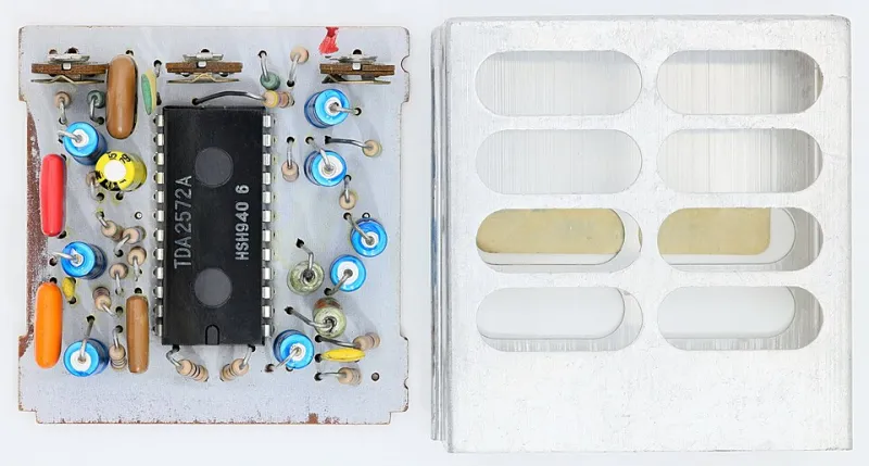
Heatsink and chassis coupling surprises engineers working with power electronics. A MOSFET's drain tab, which is often thermally bonded to a heatsink for cooling, is also electrically connected to the switching node. If the heatsink is not properly isolated or referenced, the capacitance between the switching node and the chassis creates a path for common-mode noise to propagate into adjacent circuitry or onto the AC mains—a known source of EMI compliance failures.
Simulation Strategies for Catching Parasitics Early
The most effective defense against parasitic capacitance begins before any physical prototype is built. Modern EDA tools offer several approaches to modeling these effects.
Pre-layout SPICE modeling with estimated parasitic values allows designers to explore sensitivity. By inserting small shunt capacitors at critical nodes in a schematic simulation and sweeping their values across a plausible range, engineers can identify which nodes are most vulnerable to degradation and set layout constraints accordingly.
Field solver extraction takes this further by analyzing the actual PCB geometry after layout. Tools such as Ansys SIwave, Cadence Sigrity, and the HyperLynx suite extract parasitic capacitance, inductance, and resistance from the physical layout and back-annotate these values into the simulation netlist. This post-layout simulation is considered essential practice in professional high-speed digital design and should be adopted by anyone working with signals above approximately 50 MHz.
3D electromagnetic simulation using tools like Ansys HFSS or CST Studio Suite provides the most accurate picture for RF and microwave designs, where distributed effects dominate and lumped-element approximations break down. While these tools carry significant learning curves and licensing costs, many universities and engineering schools provide access, making them a realistic option for students and researchers.
Layout Strategies That Minimize Unwanted Coupling
Simulation reveals the problem; disciplined layout practice resolves it.
The single most impactful technique is minimizing parallel trace runs between signals that must remain isolated. Routing sensitive analog lines perpendicular to digital switching lines, rather than parallel to them, dramatically reduces capacitive coupling. When parallel routing is unavoidable, increasing trace separation and inserting a grounded guard trace between the two signals provides significant isolation.
Reducing trace length at high-impedance nodes limits the area available for parasitic coupling to accumulate. In transimpedance amplifier designs used in optical receivers and sensor interfaces, keeping the feedback network as compact as possible is a standard best practice precisely because of this principle.
Via-in-pad and back-drilling techniques address the via stub problem in high-speed multilayer designs. Back-drilling removes the unused portion of a via barrel, eliminating the stub capacitance and its associated resonance. While it adds manufacturing cost, it is frequently necessary in designs operating above 5 Gbps.
Proper ground plane management—maintaining continuous, uninterrupted reference planes beneath high-speed signal layers—controls the return path geometry and keeps parasitic coupling predictable and minimal. Slots, splits, or cutouts in ground planes force return currents to detour, increasing loop area and introducing both parasitic inductance and capacitance in ways that are difficult to model after the fact.
Building the Habit of Parasitic Awareness
The most important shift for engineers at any experience level is treating parasitic capacitance not as an advanced topic to be addressed only when problems arise, but as a fundamental parameter of every physical design. Every trace has a length. Every node has a geometry. Every component sits in a three-dimensional electromagnetic environment that the schematic abstraction cannot fully capture.
Developing an intuition for where parasitic effects accumulate—and building pre-layout estimation and post-layout verification into a standard workflow—transforms parasitic capacitance from an invisible saboteur into a known, manageable design constraint. The engineers who consistently deliver first-pass prototype success are, more often than not, the ones who learned to see the circuit not just as it appears on the schematic, but as it actually exists on the board.