Keeping the Signal Clean: A Practical Guide to High-Speed PCB Design Challenges
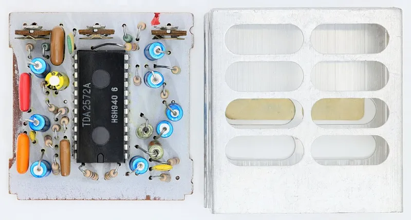
Photo: Mister rf, CC BY-SA 4.0, via Wikimedia Commons
There is a point in the evolution of every electronics designer when the comfortable abstractions of digital logic begin to break down. Wires stop behaving like wires. A trace that carries a clean square wave at one megahertz becomes an antenna, a transmission line, and a source of crosstalk all at once when the frequency climbs into the hundreds of megahertz or beyond. Welcome to the discipline of signal integrity—one of the most demanding, and increasingly essential, skill sets in modern PCB design.
With data interfaces such as DDR5, PCIe Gen 5, USB4, and high-speed SerDes links now appearing routinely in consumer electronics, industrial systems, and embedded platforms, the engineers who understand how to manage signal behavior at gigahertz speeds are in growing demand across the US electronics manufacturing sector. This article walks through the principal challenges those engineers face and the strategies they employ to overcome them.
Understanding Why High Speed Changes Everything
At low frequencies, a PCB trace is, for most practical purposes, a conductor with negligible resistance. At high frequencies, that same trace exhibits inductance, capacitance, and characteristic impedance—properties that interact with signal rise times in ways that can corrupt data, generate electromagnetic emissions, and cause functional failures that are notoriously difficult to diagnose.
The key insight is that signal integrity problems are not caused by frequency alone, but by rise time. A digital signal with a rise time of 100 picoseconds contains spectral energy well above 3 GHz, regardless of the clock rate it represents. Any physical discontinuity in the signal path—a via transition, an impedance mismatch, a reference plane gap—acts as a reflective boundary that distorts the wavefront. Understanding this relationship between rise time and effective bandwidth is foundational to thinking clearly about high-speed design.
Impedance Matching and Transmission Line Behavior
When a signal travels down a PCB trace and encounters a change in characteristic impedance, a portion of that signal reflects back toward the source. If the reflection arrives at the receiver at the wrong moment, it can corrupt the logic level the receiver is attempting to sample. This phenomenon, known as reflective noise or ringing, is one of the most common failure modes in high-speed digital systems.
Controlling impedance begins with the stackup. The characteristic impedance of a microstrip or stripline trace is determined by its width, the thickness of the copper, the dielectric constant of the PCB material, and its distance from the reference plane. Most high-speed designs target 50 ohms for single-ended traces and 100 ohms differential, though specific interface standards may specify different values. Achieving these targets requires close coordination with the PCB fabricator and, increasingly, simulation-driven stackup planning using field solver tools.
Termination strategies—series resistors placed near the driver, parallel resistors at the receiver, or AC termination networks—provide additional means of absorbing reflections that impedance control alone cannot eliminate.
Crosstalk: When Signals Interfere With Each Other
High-speed traces that run in proximity to one another exchange energy through both capacitive and inductive coupling mechanisms. This phenomenon, known as crosstalk, can inject noise onto a quiet net when an adjacent aggressor net switches. In dense PCB layouts where routing space is constrained, managing crosstalk requires deliberate spacing rules, careful layer assignment, and an understanding of how the geometry of parallel runs relates to coupling magnitude.
The standard guidance—maintain spacing of at least three times the trace width between high-speed signals, minimize the length of parallel runs, and route differential pairs as tightly coupled as possible—provides a useful starting framework. However, on designs pushing the limits of modern fabrication, rule-of-thumb approaches give way to simulation. Tools such as Ansys SIwave, Cadence Sigrity, and Mentor HyperLynx allow engineers to model crosstalk across a complete PCB layout before a board is ever fabricated, catching problems that would otherwise surface only after expensive prototype spins.
Power Delivery and Ground Plane Integrity
Signal integrity cannot be fully separated from power integrity. A power distribution network (PDN) that allows supply voltage to fluctuate as logic gates switch simultaneously introduces noise that couples directly into signal paths. Designing a low-impedance PDN—through strategic placement of decoupling capacitors, careful selection of capacitor values to target specific resonant frequencies, and solid, uninterrupted ground planes—is as important as any routing decision.
Ground plane continuity deserves particular attention. A split in a reference plane beneath a high-speed trace forces the return current to take a longer path, increasing loop inductance and generating electromagnetic emissions. One of the most common signal integrity mistakes made by less experienced designers is routing a high-speed trace across a plane split without recognizing the consequences. Maintaining uninterrupted reference planes beneath critical signals is a non-negotiable discipline.
EMI: The Regulatory and Functional Dimension
Electromagnetic interference connects signal integrity to regulatory compliance. Boards that radiate excessively may fail FCC Part 15 testing, delaying product launches and adding cost. The same design practices that improve signal integrity—controlled impedance, solid reference planes, short high-frequency loops—also reduce radiated emissions. Designers who understand this relationship can address both functional performance and compliance requirements through a unified set of layout decisions, rather than treating EMC as a separate concern addressed only at pre-compliance testing.
Shielding, filtering at board entry and exit points, and careful management of clock harmonics round out the EMI mitigation toolkit available to the PCB designer.
Building Proficiency in Signal Integrity
For students and working engineers looking to develop competency in this area, the learning path combines theory, simulation practice, and hands-on measurement experience. Acquiring access to a vector network analyzer (VNA) for S-parameter measurements, or a high-bandwidth oscilloscope with TDR capability, provides invaluable insight into how real boards behave versus how simulations predict they will behave.
The gap between those who design boards that work reliably at high speeds and those who do not is increasingly a competitive differentiator in US electronics engineering. As interface standards continue to push data rates higher and form factors continue to shrink, the demand for engineers who can keep a signal clean from driver to receiver—across a board that fits in the palm of a hand—will only intensify.